Wide-Field Scanning Electron Microscopy
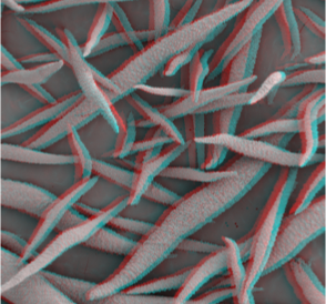
Stereo Scanning Electron Microscopy


Imaging
3D Printing
Publications
News
Gallery
Contact
Team
Research
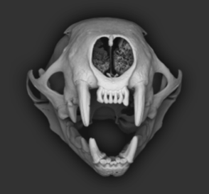
Cornell’s Wide-Field Electron Optics Laboratory specializes in the development of new Scanning Electron Microscopy imaging techniques for the high-throughput structural and compositional analysis of hierarchically ordered biological materials and synthetic constructs.
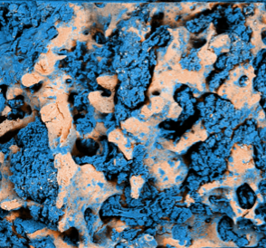
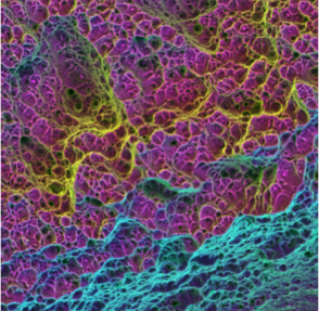
Polychromatic Scanning Electron Microscopy
Multi-Channel Energy Dispersive Spectroscopy


